EE4438 Solar Cells and Modules
Content
- Basics of semiconductors and solar cells
- I-V characteristics of illuminated solar cells
- Solar spectral energy density
- Electron-hole pair generation
- Carrier properties
- Drift and diffusive transport of electrons
- Generation and recombination
- Silicon wafer cells and thin-film cells
- Characterization
- Spectral response- Differential spectral responsivity (DSR) setup
- Resistance measurement: 4-point probe, transmission line measurements
- Effective carrier lifetime: Photoconductance & Photoluminescence imaging
- Surface texturing: Surface texturing, anti-reflective coating
- Simulation
- How solar cells are manufactured
Lab Work
For the lab, we had the chance to use the Zeiss Field Emission Scanning Electron Microscope (SEM) to detect the morphology and topography of solar cells.
The scanning electron microscope (SEM) is a characterization tool that is used to image materials up to the micro/nano-scale. Contrary to an optical microscope which focuses light on a sample, the SEM electron beam uses electron beams to interact with the sample.
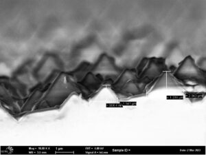
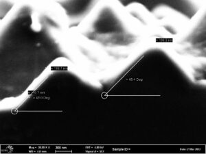
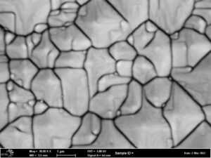
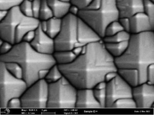
Using the SEM, we conducted top-view and cross-sectional view imaging of pyramids textured samples in using two different detectors: InLens and SE2.
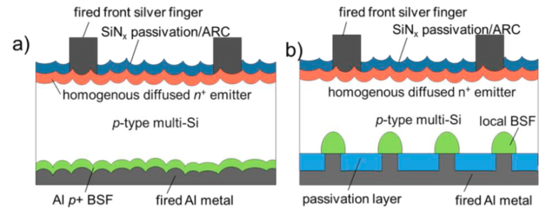
We also performed cross-sectional view imaging of screen printed full area rear contact for back surface field solar cells (Al-BSF) and local rear contact for back surface field solar cells (Al-LBSF).
The BSF is region at the back of a solar cell which is higher doped at the rear surface, causing a passivating effect on the rear surface. But Al-LBSF further improves cell performance by reducing the recombination of photogenerated electron-hole pairs at the rear surface.
